On-chip Photonics with Van der Waals Heterostructures

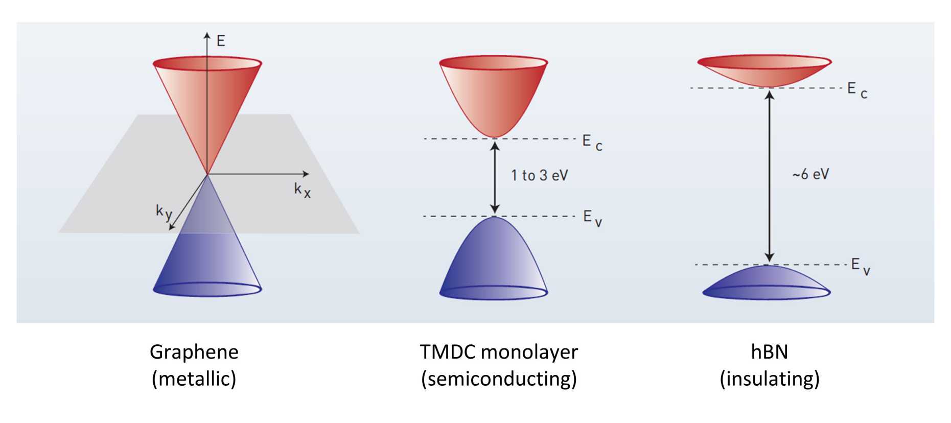
Two dimensional (2D) materials such as metallic graphene, semiconducting transition metal dichalcogenides (TMDCs) and insulating hexagonal boron nitride (hBN) have gained immense attention in the last decade as building blocks for novel integrated electronics and nanophotonics applications [1]. A unique aspect of these materials is the possibility to assemble individual layers into vertical and lateral heterostructures to create artificial materials that do not exist naturally. This opens up unprecedented opportunities for designing devices with tailored functionalities that could potentially overcome the limitations of existing technologies and revolutionize the field of optoelectronics. Moreover, owing to their planar geometry, 2D material heterostructures can be transferred onto pre-fabricated CMOS circuitry and integrated with Si photonics architectures. All these factors make them an exciting class of materials to study.
Our group conducts applied research on 2D materials with a strong focus on building optoelectronic devices such as high bandwidth photodetectors and light emitting devices (LEDs). In addition, we also develop techniques for clean transfer and fabrication of electrical contacts to these materials.
Building clean heterostructures
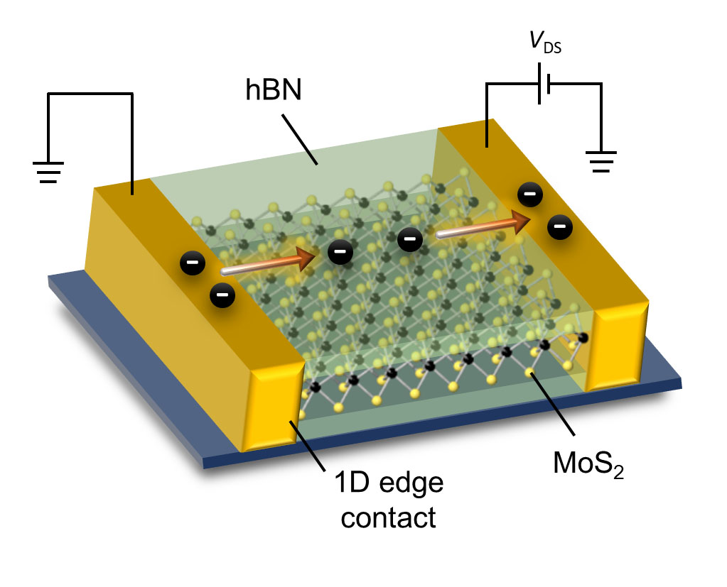
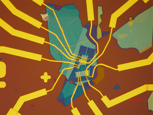
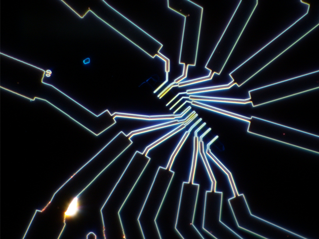
In atomically thin 2D materials, it is the surface where most physical phenomena like charge transport, light absorption/emission and van der Waals interactions happen. However, 2D material surfaces are highly susceptible to disorder arising from surface contamination, oxidation, intrinsic defects as well as the underlying substrate. Such disorder can drastically affect the electrical and optical properties of fabricated devices. For example, surface residues can trap and scatter charge carriers and also lead to a reduced luminescence quantum yield. Hence, a fundamental challenge with 2D materials is to minimize external disorder and preserve their intrinsic properties. This can be achieved by encapsulating graphene, MoS2, etc. between two sheets of hBN. To this end, we develop methods for residue free transfer and stacking of these materials [2, 3]. For gaining electrical access to encapsulated MoS2, we demonstrated that by etching through the hBN and MoS2 layers, one-dimensional edge contacts to MoS2 can be made [4]. Edge contacts can be arbitrarily narrow and scalable for building large area integrated circuits using 2D materials [4, 5].
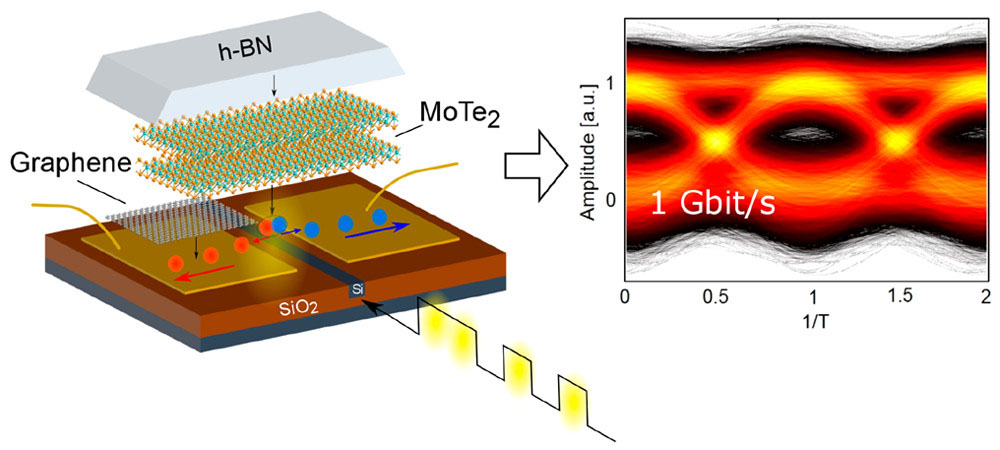
Waveguide integrated photodetectors
TMDCs possess several favorable optoelectronic properties: 1) they can possess a bandgap in the visible or near-infrared range depending on the choice of material and number of layers, 2) the bandgap is indirect in the bulk case while it becomes direct in the monolayer form and 3) they exhibit a strong light absorption per layer. This makes multilayer TMDCs an excellent choice for making photodetectors in the visible and telecom wavelength range [6]. In our group, we transfer bulk MoTe2 flakes directly onto silicon waveguides carrying optical signals. Having a large overlap area with the waveguide leads to a strong light absorption whereas by exploiting charge extraction perpendicular to the waveguide via electrodes placed nearby allows a very short transit time for the photo-generated carriers. Such a geometry results in very high speed photodetectors that can operate up to a modulation bandwidth of at least 30 GHz [7, 8]. These devices are promising for high-speed optical communications and next-generation integrated photonics circuitry.
Ultrafast, small footprint LEDs
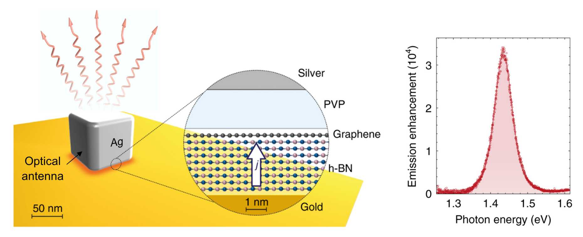
While the feature size of electronics is approaching the atomic scale, the footprint of optical devices is typically bound by the wavelength of light. This mismatch in length scales is currently two to three orders of magnitude. New strategies and materials are required to shrink the size of optical devices to the deep subwavelength scale in order to co-integrate photonic and electronic circuitry and for transmitting information between different nodes. This is where optical antennas come in: their resonant optical response gives rise to strongly enhanced and localized fields that can be utilized for boosting the local light-matter interaction and thereby reduce device footprint [9]. However, traditionally optical antennas have been mostly excited by external light sources whereas electrically driven optical antennas are a prerequisite for on-chip light generation [10].
In this regard, 2D materials and their heterostructures provide a unique platform for engineering light emission on the nanometer scale – both in the visible and near-infrared spectral range. By coupling 2D materials with suitable optical antenna structures such as silver nanocubes (see figure), we are building small footprint light sources [11-12], with demonstrated operating speeds of up to 1 GHz [11]. In atomically thin 2D materials, the volume available for light-matter interactions is small. Optical antennas not only enhance the interaction volume and increase the efficiency of light emitting devices, but also enable efficient out-coupling of the generated light [13-14] and steering of the emission direction [15]. This ultimately allows ultrafast generation of light from a small area dictated by the antenna size (< 100 nm x 100 nm ideally).
Apart from optical antennas, bulk 2D materials can themselves be used as dielectrics to confine optical fields below the bandgap. By patterning bulk 2D dielectrics into nanostructures such as disk resonators, cavities and waveguides transmission/absorption resonances can be engineered to enhance light matter interaction at certain wavelengths and for in-plane light guiding. This is also something our group is actively investigating, with several open challenges still remaining.
Optical memristors
A memristor is a device whose resistance depends on the history of the voltages that have been applied to it, i.e. a resistor that shows hysteresis. Memristors have been proposed as potential building blocks for future neuromorphic (brain-like) computing architectures. In our group, we are working on building memristors made using TMDCs like MoS2, with the objective of probing and controlling their memristive behavior optically.
Related publications
[1] P. Bharadwaj and L. Novotny, Optoelectronics in Flatland. Optics and Photonics News 26, 24-31 July/August (2015).
[2] M. Her, R. Beams and L. Novotny, Graphene transfer with reduced residue. Phys. Lett. A 377, 1455-1458 (2013).
[3] A. Jain et al., Minimizing residues and strain in 2D materials transferred from PDMS. Nanotechnology 29, 265203 (2018).
[4] A. Jain et al., One-dimensional edge contacts to a monolayer semiconductor. Nano Letters 19, 6914-6923 (2019).
[5] Á. Szabó et al., Electron Transport through Metal/MoS2 Interfaces: Edge- or Area-Dependent Process? Nano Letters 19, 3641-3647 (2019).
[6] N. Flöry et al., A WSe2/MoSe2 heterostructure photovoltaic device. Appl. Phys. Lett. 107, 123106 (2015).
[7] P. Ma, N. Flöry et al., Fast MoTe2 waveguide photodetectors with high sensitivity at telecommunication wavelengths. ACS Photonics 5, 1846 (2018).
[8] N. Flöry et al., Waveguide-integrated van der Waals heterostructure photodetector at telecom band with high speed and high responsivity. Nature Nanotech. 15, 118-124 (2020).
[9] L. Novotny and N. F. Hulst. Antennas for light. Nature Photon. 5, 83-90 (2011).
[10] R. Beams, P. Bharadwaj, L. Novotny. Electroluminescence from graphene excited by electron tunneling. Nanotechnology 25, 055206 (2014).
[11] M. Parzefall et al., Antenna-coupled photon emission from hexagonal boron nitride tunnel junctions. Nature Nanotech. 10, 1058 (2015).
[12] M. Parzefall et al., Light from van der Waals quantum tunneling devices. Nature Commun. 10, 292 (2019).
[13] M. Parzefall and L. Novotny. Light at the end of the tunnel. ACS Photonics 5, 4195-4202 (2018).
[14] M. Parzefall and L. Novotny. Optical antennas driven by quantum tunneling: a key issues review. Rep. Prog. Phys. 82, 112401 (2019).
[15] S. Busschaert et al., Beam steering with a nonlinear optical phased array antenna. Nano Letters 19, 6097-6103 (2019).