Nanocarbon Photonics
The objective of this project is to control and understand the influence of defects and dopants on the physical properties of carbon nanotubes and graphene.
The intentional generation of defects and dopants in carbon nanotubes and graphene provides an opportunity to engineer electronic and structural properties, similar to semiconductor devices. For example, in semiconductors electron concentration and electrical conductivity can be varied over six orders of magnitude by varying doping densities. Furthermore, optical emission time constants and quantum efficiencies can be varied over four to five orders of magnitude by varying defect concentrations. Virtually every practical application of semiconductors relies on the effects of dopants, defects, and interfaces. Similarly, it can be expected that defects and dopants will have a strong influence on future ‘nanocarbon’ devices.
In this project we apply high-resolution spectroscopic imaging techniques to further our understanding of the optoelectronic properties of nano carbon materials. Vice versa, we exploit the unique properties of graphene and carbon nanotubes to achieve new device functionality. While pristine nanotubes and graphene have been thoroughly explored, many potential applications require the introduction of defects into the lattice to engineer desired electrical and optical characteristics.
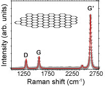
The Raman scattering spectrum of graphite is known to exhibit several peaks that are only observed in the presence of structural defects in the hexagonal lattice. The same peaks are also observed in carbon nanotubes and graphene. Of particular interest is the D band (~1350cm-1) that appears close to the first-order allowed peak denoted as G band (~1580 cm-1). Electrons involved in the double-resonance process giving rise to the D band are inelastically scattered by phonons in the interior of the first Brillouin zone. However, because of momentum conservation these phonons can only become Raman active if the electrons involved in the process are elastically scattered by a defect. The intensity ratio between the disorder-induced D band and the G band is widely used as a measure for the average crystallite size in graphitic systems.
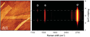
The graphene edge forms a model defect, which allows us to systematically investigate the localization of the Raman D band (see image above). Using an optical defocusing method we can achieve a resolution of a few nanometers. As the temperature is decreased from 300 to 1.55 K, the D band localization length lD increases. Our measurements reveal that the localization of the D band varies as 1/√T, giving strong evidence that lD scales with the coherence length of photoexcited electrons and holes near graphene edges.
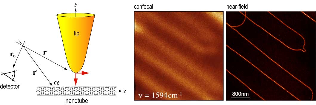
To zoom-in on single defects and dopants we use tip-enhanced Raman scattering (TERS). As shown in the image below, this method uses a metal tip as an optical antenna to localize and enhance incident laser radiation and to interact locally with nanocarbon materials. The technique makes it possible to measure local electronic and structural properties with a spatial resolution of ~ 10nm and has been used to record high-resolution spatial maps of optically active phonons and localized photoemission.
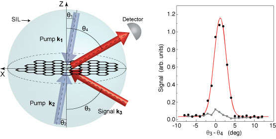
One application is phase conjugation, - a four-wave mixing process in which the phase of one of the input beams is reserved. We have used this effect to demonstrate controllable negative refraction at a graphene interface. The experiment uses two pump beams (blue arrows) that are focused on a graphene flake at angles θ1= θ2 writing a holographic grating (see figure below). A signal beam (lower red arrow) is refracted in negative direction (upper red arrow) and is detected by a photodetector. The graphene sample has been sandwiched between two hemispherical SILs to provide a rotational symmetry to the sample. The data shown below shows that the signal beam is indeed refracted in negative direction, which opens up the possibility to perform super-resolution imaging with low loss and over a large spectral bandwidth.
Related publications:
[1] R. Beams, L. G. Cancado, and L. Novotny, ”Low temperature Raman study of the electron coherence length near graphene edges ,” Nano Lett. 11, 1171-1181 (2011).
[2] L. G. Cancado, A. Jorio, A. Hartschuh, A. Ismach, E. Joselevich, and L. Novotny, ”Near-field Raman enhancement in one-dimensional systems,” Phys. Rev. Lett. 103, 186101 (2009).
[3] I. O. Maciel, N. Anderson, M. A. Pimenta, A. Hartschuh, H. Qian, M. Terrones, H. Terrones, J. Campos-Delgado, A. M. Rao, L. Novotny, and A. Jorio, ”Electron and phonon renormalization at defect/doping sites in carbon nanotubes,” Nature Materials 7, 878 - 883 (2008).
[4] H. Qian, C. Georgi, N. Anderson, A. A. Green, M. C. Hersam, L. Novotny, and A. Hartschuh, ”Exciton energy transfer in pairs of single-walled carbon nanotubes,” Nano Lett. 8, 1363-1367 (2008).
[5] N. Anderson, A. Hartschuh, and L. Novotny, “Chirality changes in carbon nanotubes studied with near-field Raman spectroscopy,” Nano Lett. 7, 577-582 (2007).
[6] A. Hartschuh, H. Pedrosa, L. Novotny, and T. D. Krauss “Simultaneous fluorescence and Raman scattering from single carbon nanotubes,” Science 301, 1354–1357 (2003).
[7] A. Hartschuh, E. J. Sanchez, X. S. Xie, and L. Novotny, “High-resolution near-field Raman microscopy of single-walled carbon nanotubes,” Phys. Rev. Lett. 90, 95503 (2003).